Contents
Overview
The genesis of chip fabrication engineering can be traced back to the invention of the transistor at Bell Labs in 1947 by John Bardeen, Walter Brattain, and William Shockley. This foundational discovery paved the way for the integrated circuit, first demonstrated by Jack Kilby at Texas Instruments in 1958 and independently by Robert Noyce at Fairchild Semiconductor in 1959. Early fabrication relied on germanium, but Gordon Moore and Irvine Grange at Fairchild championed silicon in the early 1960s, a material that would dominate the industry. The development of photolithography, a technique adapted from printing, became the cornerstone for patterning circuits, with early pioneers like Jean Hornby and Dan Maydan at Fairchild and later Applied Materials refining these processes. The establishment of dedicated foundry models, where companies like TSMC (Taiwan Semiconductor Manufacturing Company) began producing chips for fabless design firms in the late 1980s, fundamentally reshaped the industry's structure.
⚙️ How It Works
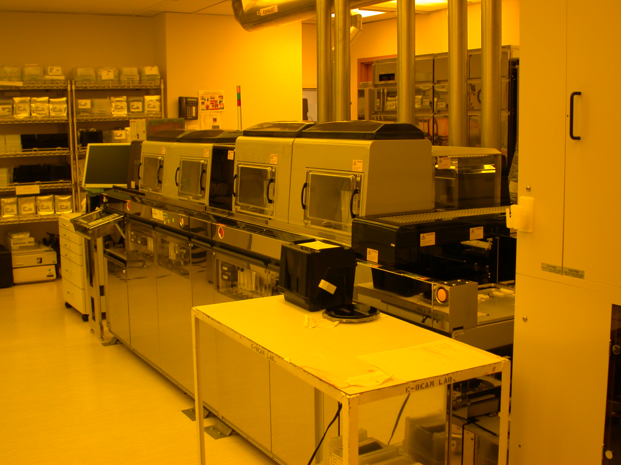
Chip fabrication is a meticulously orchestrated sequence of hundreds of steps, primarily occurring within Class 1 or better cleanrooms to prevent particulate contamination. The process begins with a pure silicon wafer, typically 300mm in diameter. Photolithography is central, using ultraviolet light to transfer circuit patterns from a mask onto a light-sensitive photoresist coating the wafer. Etching processes, either wet chemical or dry plasma-based, then selectively remove material to define the circuit features. Deposition techniques, such as chemical vapor deposition (CVD) and physical vapor deposition (PVD), are used to add thin films of various materials, including insulators like silicon dioxide and conductors like copper. Ion implantation precisely introduces dopant atoms into specific regions of the silicon to alter its electrical conductivity, creating transistors and other components. These steps are repeated dozens of times to build up the complex, multi-layered architecture of modern ICs, with each layer requiring sub-nanometer precision.
📊 Key Facts & Numbers
The global semiconductor manufacturing market is colossal, projected to reach over $1 trillion by 2030, a significant leap from approximately $580 billion in 2022. Leading-edge fabrication facilities, known as fabs, cost upwards of $20 billion to build and equip, with TSMC and Samsung Electronics operating some of the most advanced plants. A single 300mm silicon wafer can yield hundreds or even thousands of individual chips, depending on their complexity and size. The smallest features on leading-edge chips, such as those produced at Intel's or TSMC's 3nm nodes, are measured in single-digit nanometers (billionths of a meter). The yield rate—the percentage of functional chips per wafer—is a critical metric, with even a 1% improvement translating into millions of dollars in savings. The average fabrication time for a cutting-edge chip can stretch to 15 weeks, highlighting the intricate and time-consuming nature of the process.
👥 Key People & Organizations
Key figures in chip fabrication engineering include Gordon Moore, co-founder of Intel, whose eponymous law predicted the exponential growth of transistor density. Jack Kilby and Robert Noyce are credited with inventing the integrated circuit. Dan Maydan is a pivotal figure in the development of deposition and etch equipment at Applied Materials. Morris Chang, founder of TSMC, pioneered the pure-play foundry business model. Major organizations driving fabrication include Intel, Samsung Electronics, and TSMC, which dominate advanced manufacturing. ASML Holding is a critical player, holding a near-monopoly on the extreme ultraviolet (EUV) lithography machines essential for producing the most advanced chips. GlobalFoundries and UMC are other significant foundry players.
🌍 Cultural Impact & Influence
Chip fabrication engineering is the invisible engine of the digital age, underpinning virtually every modern technology. The miniaturization and increasing power of ICs, driven by fabrication advancements, have enabled the proliferation of personal computers, smartphones, the internet, and artificial intelligence. The cultural impact is profound: from the entertainment we consume on Netflix to the communication facilitated by WhatsApp, our daily lives are inextricably linked to the chips produced through these processes. The economic influence is equally vast, with the semiconductor industry being a cornerstone of global trade and technological competitiveness, driving innovation across sectors like automotive, healthcare, and aerospace. The very concept of Moore's Law, a direct consequence of fabrication progress, has shaped technological expectations for decades.
⚡ Current State & Latest Developments
The current state of chip fabrication is defined by an intense race for technological supremacy, particularly in sub-10nm process nodes. ASML's introduction of EUV lithography has been a game-changer, enabling finer feature sizes and higher yields for advanced chips. Geopolitical tensions are also significantly impacting the industry, with governments worldwide investing heavily in domestic chip manufacturing capabilities through initiatives like the CHIPS Act in the United States and similar programs in Europe and Asia. This has led to a surge in new fab construction, including major investments by Intel in Arizona and Ohio, and TSMC in Arizona and Japan. The industry is also grappling with supply chain resilience and the increasing cost and complexity of developing next-generation manufacturing technologies.
🤔 Controversies & Debates
The primary controversy in chip fabrication revolves around the immense cost and environmental impact of building and operating fabs. The sheer volume of water and energy consumed, along with the use of hazardous chemicals, raises significant sustainability concerns. Furthermore, the concentration of advanced manufacturing in a few key regions, particularly Taiwan, creates geopolitical vulnerabilities and supply chain risks, as highlighted by the ongoing global chip shortage. Debates also persist regarding the economic viability of continuing Moore's Law, with some arguing that the cost of scaling to smaller nodes is becoming prohibitive, leading to a slowdown in the historical pace of improvement. The ethical implications of the industry's reliance on complex global supply chains and potential labor issues in manufacturing are also subjects of scrutiny.
🔮 Future Outlook & Predictions
The future of chip fabrication points towards continued innovation in materials science and process technology. Beyond silicon, research into gallium nitride (GaN) and silicon carbide (SiC) is accelerating for power electronics, while carbon nanotubes and graphene are being explored for future transistor generations. Quantum computing may eventually require entirely new fabrication paradigms. The integration of AI into the design and manufacturing process itself is expected to optimize yields, reduce development times, and enable more complex chip architectures. The trend towards specialized chips for AI, IoT, and automotive applications will likely drive further diversification in fabrication techniques and materials. Expect continued consolidation and strategic partnerships as companies navigate the escalating costs and complexity of leading-edge manufacturing.
💡 Practical Applications
Chip fabrication engineering is directly applied in the production of virtually all modern electronic devices. This includes the CPUs and GPUs fou
Key Facts
- Category
- technology
- Type
- topic